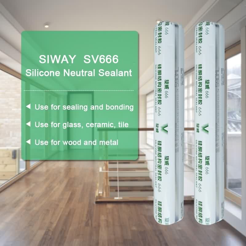
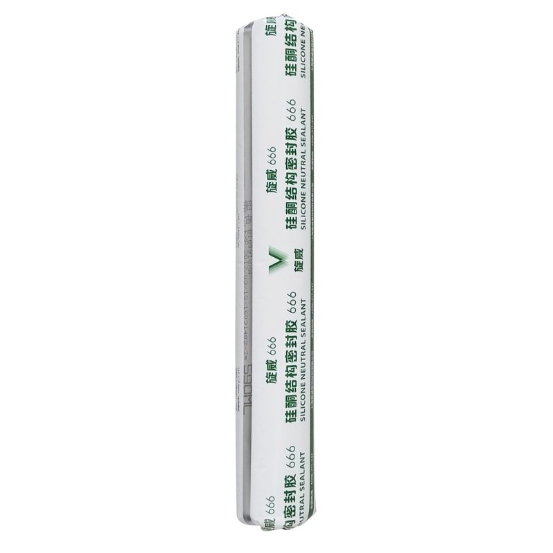
Factory best selling SV-666 General Use Neutral Sealant for Lisbon Factory
Short Description:
Description SV-666 neutral silicone sealant is a neutral curing glue single component, the modulus of the. It is specially designed for windows and doors caulking sealing general plastic doors and windows. It has good adhesion to glass and aluminum alloy, and has no corrosion. Where to use It is fit for multiple purpose sealing and bonding applications to form a silicone rubber adhering to adjacent substrates e.g. glass, ceramic, tile, wood and metal. Key Features 1. 100% silicone 2. Eas...
We are proud of the high customer satisfaction and wide acceptance due to our persistent pursuit of high quality both on product and service for Factory best selling SV-666 General Use Neutral Sealant for Lisbon Factory, We sincerely welcome you come to visit us. Hope we have good cooperation in the future.
Description
SV-666 neutral silicone sealant is a neutral curing glue single component, the modulus of the. It is specially designed for windows and doors caulking sealing general plastic doors and windows. It has good adhesion to glass and aluminum alloy, and has no corrosion.
Where to use
It is fit for multiple purpose sealing and bonding applications to form a silicone rubber adhering to adjacent substrates e.g. glass, ceramic, tile, wood and metal.
Key Features
1. 100% silicone
2. Easy to use
3. Waterproofing and weatherproofing
4. Primerless adhesion to most building materials
5. 12.5% movement capability
Technical data sheet
| Test standard | Test project | Unit | value |
| Before curing——25℃,50%R.H. | |||
| GB13477 | Flow, sagging or vertical flow | mm | 0 |
| GB13477 | surface drying time(25℃,50%R.H.) | min | 30 |
|
GB13477 |
Operating time | min | 20 |
| Curing time(25℃,50%R.H.) | Day | 7-14 | |
| Sealant curing speed and operating time will have different with different temperatures and temperature, high temperature and high humidity can make sealant curing speed faster, rather low temperature and low humidity are slower.21 days after curing——25℃,50%R.H. | |||
| GB13477 | Durometer Hardness | Shore A | 28 |
| GB13477 | The ultimate tensile strength | Mpa | 0.7 |
| Temperature stability | ℃ | -50~+150 | |
| GB13477 | Movement capability | % | 12.5 |
Certification
JC/T881-2001 12.5E;GB/T14683-2003 12.5E
Color
Black,White,Gray
Package
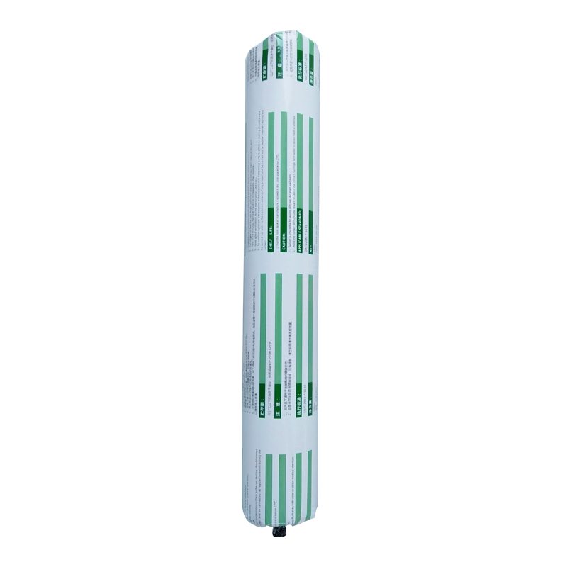
300ml in cartridge * 24 per box, 590ml in sausage *20 per box
Shelf life
12 months
Note
If you want the TDS or MSDS or other details, please contact with our sales person.
This simple animation video clearly explains the topics P-N junction semi conductor or diode, what is forward bias and reverse bias, what is diffusion current and drift current, what is avalanche breakdown etc
What is a P — N junction semiconductor and how is it formed?
The PN junction semi conductor is a combination of P type semiconductor with N type semiconductor to achieve the practical utility of both. It’s formed, when a P type semi conductor is joined to an N type semiconductor.
The P type semiconductor has free holes with positive charged and the N type semiconductor has free electrons with negatively charge.
What happens when a PN junction is made?
When P and N semiconductors are joined to make the PN junction semiconductor diode, the electrons near the PN junction jump from N to P and holes near the junction jump from P to N. This phenomenon creates a space charge region or a depletion layer as shown in the video. At this space charge region due to the movement we have electrons in P region and holes in N region. For some time the electrons move back from P to N in the space region or depletion layer and some holes move back from N to P in the space region. This continues to happen till equilibrium is reached. This movement of electrons and holes in the space region or diffusion layer gives rise to Diffusion current.
What is Forward bias and how does it occur?
Forward bias occurs when the positive terminal of battery is connected to the P region and the negative terminal of battery is connected to the N region. In this condition what happens is the positive terminal repels the holes towards the junction and the negative terminal repels the electrons towards the junction. Due to this repulsion, the depletion region or space region narrows down as shown in the video.
But at a particular condition, If the voltage in the forward bias is above a specified range, the electrons in the N region drifts through the junction and migrates to the P region and the holes in the P region drifts through the junction and migrates to the N region.
Now the current flows across the circuit and this current are called the Drift current.
What is Reverse bias and how does it occur?
Reverse bias occurs when the negative terminal of the battery is connected with the N region and positive terminal with the P region. In this condition holes (positively charged) from the P region get attracted to the negative terminal of the battery and electrons (negatively charged) get attracted to the positive terminal of the battery. This results in the depletion layer to widen up.
Now the PN junction acts as an insulator and will not allow any current to flow in the circuit. But at a condition, if the battery voltage is above a particular limit, which is called as the reverse bias breakdown voltage level. Electrons and the holes breakdown through the PN junction and cross over resulting in the current to flow through the circuit. This break down is called avalanche breakdown
In this process the current flowing through the PN junction is very high and ultimately the PN junction gets damaged due to overheating caused by the excess flow of current.
This is how a PN junction semiconductor works.
——-
As you all know there are many technical video been uploaded on our YouTube channel https://www.youtube.com/user/TechTrixInfo you can also watch these video from our web site www.TechTrixInfo.com
These are some of our famous tutorial video:
How to drive n Operate a JCB BHL Machine: https://www.youtube.com/watch?v=d0QsBcyuQKw&list=TLxVT-8RVZwj6rt8TF6qQASojgB2HyFj6A
How piston pump works: https://www.youtube.com/watch?v=BEpQFZ5BG8c
Animation – How Clutch Works: https://www.youtube.com/watch?v=H7Iay0Ke_t4&list=TLEAR3w8CXdzQVx8Wk-RWxgIKniXTYNllp
How fuel injection pump works: https://www.youtube.com/watch?v=HVIE36oIR1s&list=TLbG7_oGzfXfRpBh5Sa-6bA0OGexW_wY2T
How Hydraulic Ram Works: https://www.youtube.com/watch?v=svdsbL4PLL4&list=TLsKtRNvm03sqKvd1AwOEbOsWZZezoXJ5z
We are also having a drawing video tutorial channel: https://www.youtube.com/user/EthansHowToDaw
Answer to all the below questions are available in this video:
How pn junction diode works. How diode works, animation diode, animation pn junction, working of pn junction, how does a pn junction semiconductor works, what is avalanche breakdown, what is drift current, how drift current forms, what is space charge region, how space charge region forms, what is depletion layer, how depletion layer formed, how an electric field is formed in pn junction, what is forward bias, what is reverse bias, how forward bias occurs, how reverse bias occurs, what is diffusion current, how diffusion current is formed.